




 Share
Share







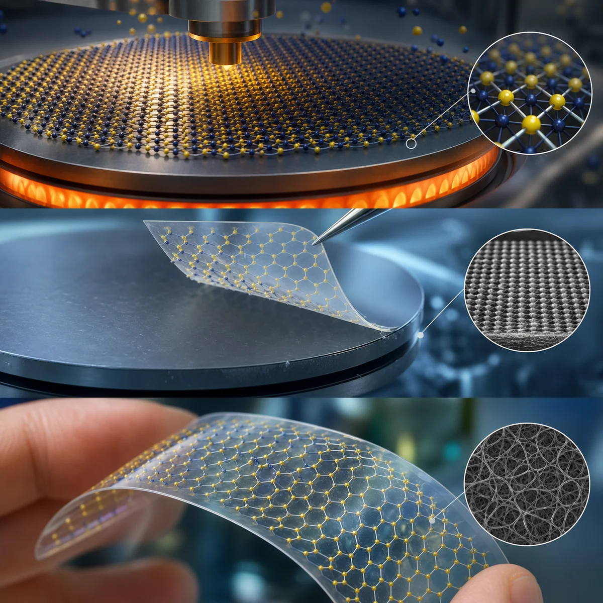
Flexible electronics face a manufacturing contradiction. High-quality semiconductor materials often need processing temperatures that ordinary plastic cannot survive, yet plastic is exactly what lets a finished device bend. Stanford engineers separated those steps. They grew an atomically thin semiconductor on heat-tolerant silicon, completed the demanding fabrication there, cooled the structure, and transferred it onto a flexible plastic base.
The active semiconductor film was only three atoms thick. That extreme thinness helped the transistor flex while retaining high performance, and the transfer method avoided cooking the final plastic substrate. Instead of asking every material to tolerate the same factory conditions, the process let each one enter when it could handle the work: silicon for heat, plastic for bending.
The headline needs one important layer of restraint. The complete transistor and circuit stack was not three atoms thick; that measurement describes the semiconductor film inside it. The result was also a fabrication advance demonstrated by engineers, not a flexible consumer screen ready for purchase. Its significance is architectural: build delicate electronics on a temporary rigid host, then move the useful layer to the surface where flexibility matters.
Sources